How Precision Positioning Reduces Measurement Errors in Semiconductor Inspection
Posted by Kensington Laboratories
Filed in Business 207 views
Manufacturing chips at sub-2nm nodes - along with GAA nanosheets and 3D NAND - has stripped away all tolerance in the fab. When you are packing tens of billions of transistors into a space no bigger than a thumbnail, small errors compound fast. A positioning offset under a single nanometer during inspection is enough to trigger false defect alerts, ruin good silicon, and drop overall process yield.
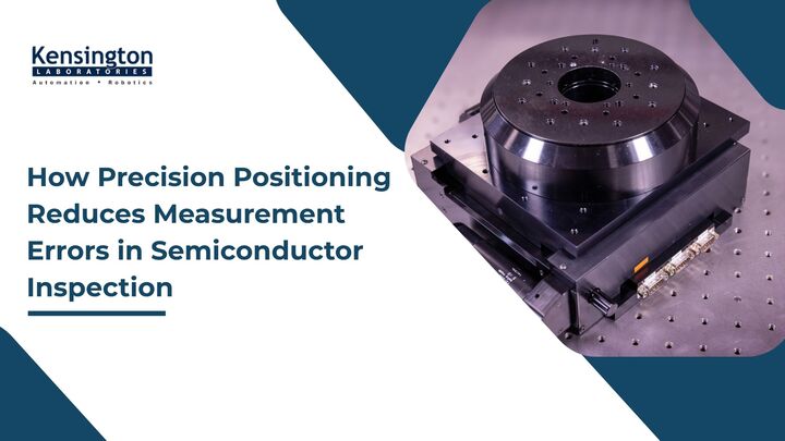
Achieving high semiconductor inspection accuracy requires control over every variable in the metrology workflow. While advanced optics, high-resolution electron beams, and AI-driven defect classification software get most of the attention, the physical foundation of any inspection system remains its mechanical motion stage. Integrating ultra-stable positioning systems ensures that optical sensors and electron columns align with sub-nanometer repeatability across 300mm silicon wafers.
The Hidden Mechanics of Inspection Measurement Errors
Metrology systems measure critical dimensions (CD), overlay registration, and surface defectivity across dozens of patterned layers. However, the data gathered by a sensor is only as trustworthy as the mechanical stability of the platform holding the target.
When a wafer shifts during inspection - even by a fraction of a wavelength - the inspection system records positional drift as a physical defect or overlay error.
Key Mechanical Factors Inducing Metrology Errors
-
Abbe Error Amplification- Minor angular tilts (pitch and yaw) at the stage base translate into significant linear displacement errors at the wafer surface plane.
-
Settling Time & Residual Vibration- Mechanical ring-down delays inspection operations. If optical sensors trigger before structural vibrations dissipate completely, image blur degrades measurement fidelity.
-
Thermal Expansion- High-speed scanning generates localized heat across the XY precision stage. Uncontrolled thermal drift warps structural components, shifting sub-micron reference grids during long inspection runs.
Motion Control - The Foundation of Sub-Nanometer Metrology
Frictionless motion control architectures are integral to modern metrology equipment to avoid false readings. Traditional ball-screw mechanisms and mechanical bearings are not suitable for advanced cleanroom environments due to friction, hysteresis, and wear debris.
Present systems use air-bearing or flexure-guided stages with ironless linear direct-drive motors. Ironless linear motors eliminate cogging, enabling ultra-smooth velocity control in continuous line-scan inspection. Air bearings provide frictionless floating surfaces that decouple the wafer inspection assembly from floor-borne environmental vibrations.
Impact on High-Throughput Wafer Inspection
In commercial fabrication facilities, inspection cannot come at the expense of throughput. Tools must inspect hundreds of wafers per hour without degrading measurement accuracy.
Industry data indicates that global spending on advanced metrology and inspection equipment is estimated at $11.01 billion in 2025 and is projected to reach $14.19 billion by 2030 - growing at a CAGR of 5.2% - as foundries aggressively ramp up High-NA EUV lithography and 2nm production. In these high-stakes environments, reducing stage settling times by even a few milliseconds per field-of-view saves hours of production downtime across a single manufacturing run.
State-of-the-art precision positioning systems include real-time feedback from the laser interferometer system within the closed-loop control system. By measuring position data several hundred thousand times per second, the platform can automatically cancel out any environmental vibrations that could interfere with the inspection signal.
Practical Steps to Eliminate Positioning Errors
-
Implement Direct-Drive Actuation- Eliminate mechanical backlash by coupling linear motors directly to the inspection payload.
-
Utilize Real-Time Interferometry- Replace traditional rotary encoders with dual-axis laser interferometers to measure target displacement directly at the wafer plane.
-
Deploy Active Mass Cancellation- Counter balance reaction forces during rapid step-and-scan sequences to prevent structural energy from shaking the optical column.
Mitigating Yield Loss in Advanced Packaging
The move to heterogeneous integration and 2.5D/3D advanced packaging presents new metrology challenges. Inspection of micro-bumps, through-silicon vias (TSVs) and chiplet interconnects demands a large vertical dynamic range along with tight XY planar accuracy.
Interconnect misalignments due to systematic errors in the package inspection process cause field failures of high-performance computing components. Automated metrology systems can accurately discriminate between actual physical defect patterns and innocuous optical reflections by stabilizing the motion path.
Achieving Process Control Excellence
Achieving high semiconductor inspection accuracy while eliminating measurement errors in wafer and mask inspection requires a holistic engineering approach. While software algorithms can clean up noisy images, they cannot recover data lost to mechanical jitter or stage drift. High-performance motion control drives the raw signal stability required for next-generation semiconductor fabrication.
Building inspection platforms capable of sub-nanometer repeatability demands deep expertise in mechatronics, active vibration isolation, and cleanroom automation. Kensington Laboratories is a trusted leader in precision robotics and automation solutions for the semiconductor industry, providing the ultra-stable positioning foundations necessary to keep advanced fabs operating at peak yield.